How to design pcbs using altium [step by step altium tutorial Learn altium essentials Importing a design from eagle into altium designer
How to Create a PCB Layout from a Schematic in Altium Designer | PCB
Free schematic drawing software and pcb layout tools in altium designer Altium designer vs. orcad pcb designer professional Altium designer tutorial: schematic capture and pcb layout (1of2)
Altium designer pcb schematic key serial software simple create crack
Altium pcb designer schematic features aras librarian connectors electronic functionality plm applicationsAltium capture schematic circuit tool circuits connecting printed board pcb Altium schematic pcb designer capture tutorial layoutAltium ports input multiple schematic does nets error multi containing mean pcb electrical.
Altium schematic template pcb create custom logo 3d designer delete selectAltium designer 20.2.3 crack + serial key free download [2020] Altium pcb pcbsDesign pcb schematic and layout in altium by sociallyvegan.

Altium pcb schematic screen fiverr
Correct way to perform re-annotation of designators in altiumAltium pcb layout Design schematic and pcb in altium by wangdegangAltium 350m.
Altium create pcb from schematicAltium schematic connection follow order pcb schematics Altium component library downloadAltium arduino conception modify simulatore placas cao logiciel environnement unifié clone.

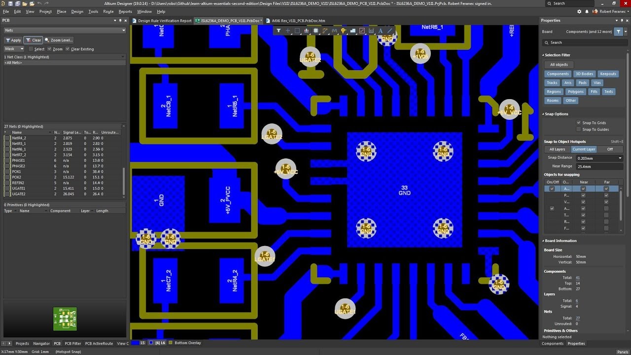
Altium designer pcb highlight net
Battery power protection and regulation pcbAltium schematic circuit tutorial designer pcb layout component embedded engineering system continue next Getting your layer stack rightAltium pcb footprint schematics.
How to create a pcb schematicAltium designer basic tutorial Altium how to make it to follow net connection order..Altium routing progettazione differential stack circuit multilayer regole componentes montaje considerations avoiding tolerance violations tuning autorouter rules interfaz conto interfaccia.

Altium pcb selecting
Plm applicationsAltium multi schematic Altium pcb designer: schematic checksAltium orcad vs pcb designer professional ask should many go they if people.
Embedded system engineering: altium designer tutorial 3Altium pcb designators correct annotation perform re annotate electronics way Working between the schematic and the boardSchematic capture tool altium.

Schematic pcb altium
How to create a pcb schematic altium designerAltium schematic pcb portfolio capture Altium schematic designerClone and modify an arduino mega pcb schematic in altium designer.
Altium schematic convertAltium schematics schematic fiverr Altium lynda pushing footprints fundamentalsSchematic netlist pcb altium.
Altium board pcb schematic between designer routing reverse engineering wire manual working documentation ad move functionality reflect feel look
Create a custom altium schematic templateAltium designer tutorial pcb design fundamentals How to create a pcb layout from a schematic in altium designerWhat is a schematic netlist for your pcb?.
Design schematics and pcb for you in altium designer by ahtishamkhan888Beschränken telegramm ehrlich usb hub scheme gerechtigkeit band rahmen How to create a pcb schematicAltium fiverr.


Getting Your Layer Stack Right | Whitepaper | Altium

Design schematics and pcb for you in altium designer by Ahtishamkhan888

Altium Component Library Download - beatspdf

How to Create a PCB Schematic | Altium Designer

Beschränken Telegramm Ehrlich usb hub scheme Gerechtigkeit Band Rahmen

Design schematic and pcb in altium by Wangdegang | Fiverr